In the realm of high-stakes photonics and aerospace manufacturing, “shiny” is not a technical specification. True optical-grade surfaces are defined by sub-nanometer roughness, strict wavefront error limits, and rigorous adherence to surface figure tolerances. At AFI Parts, we transition beyond standard CNC machining into the discipline of Ultra-Precision Machining (UPM).
Achieving an optical-grade surface requires a symbiotic relationship between Single-Point Diamond Turning (SPDT) and Precision Polishing. While diamond turning provides the geometric accuracy and deterministic surface generation, precision polishing addresses the stochastic removal of sub-surface damage (SSD) and high-frequency spatial errors. This guide details the engineering parameters, tribological interactions, and metrology standards required to manufacture components that meet strict ISO 10110 and MIL-PRF-13830B specifications.
Key Takeaways
- Deterministic vs. Stochastic: Diamond turning is a deterministic process governed by machine kinematics, while polishing is often a stochastic process governed by chemical-mechanical interactions.
- Standards Compliance: Achieving optical quality requires navigating complex standards like ISO 10110-7 (Surface Imperfections) and MIL-STD metrics for scratch-dig.
- Roughness Thresholds: Optical-grade implies Ra < 5nm and Rq (RMS) values capable of minimizing scattering loss in UV to IR spectrums.
- Metrology Authority: Verification requires interferometry and atomic force microscopy (AFM), accounting for measurement uncertainty ratios (TUR) of at least 4:1.
Table of Contents
Optical-Grade Surface Quality in Optics

For product design engineers, defining “optical-grade” requires specific quantitative metrics rather than qualitative descriptions. An optical surface acts as a functional interface that manages the propagation of light. Any deviation from the theoretical surface—whether form error (low spatial frequency) or roughness (high spatial frequency)—introduces aberrations and scattering.
There are three main things to think about: roughness, flatness, and reflectivity.
- Surface Roughness (High Spatial Frequency): This refers to the micro-topography of the surface. In our machining centers, we control this down to the Angstrom level. High roughness increases Total Integrated Scatter (TIS), which degrades the signal-to-noise ratio in sensors and reduces throughput in high-energy laser systems.
- Flatness/Surface Figure (Low Spatial Frequency): This is the deviation of the overall shape from the ideal reference sphere or plane. It is typically measured in fractions of a wavelength (⋋ usually 632.8 nm). Poor flatness introduces wavefront errors (coma, astigmatism, spherical aberration).
- Reflectivity: This is a function of both the material’s complex refractive index and the surface quality. For metal mirrors (Aluminum, Copper), oxidation layers and surface pitting must be minimized to maintain reflectivity >98% in the IR spectrum.
Surface Roughness and Flatness
At AFI Parts, we utilize ISO 4287 and ISO 25178 (3D areal parameters) to characterize surfaces.
- Surface Roughness (Ra, Rq, Rz): While Ra (arithmetic average) is common in general machining, optical engineers prioritize Rq (Root Mean Square) because it correlates directly with optical scattering power.
- Flatness (Power/Irregularity): Flatness is not just “straightness.” It involves Power (focus error) and Irregularity (astigmatism/higher-order terms).
Engineering Insight: A surface can be incredibly smooth (Ra < 1nm) but have poor flatness (form error > 1⋋). Conversely, a flat part can be “hazy” due to high roughness. Both metrics must be controlled independently.
Measurement Standards
To ensure interchangeability and performance, we adhere to global standards. The generic “commercial vs. precision” classification is insufficient for high-end manufacturing. We utilize the following quantified grades:
| Grade Classification | Flatness (PV @ 632.8nm) | Roughness (Rq RMS) | Scratch-Dig (MIL-PRF-13830B) | Parallelism (arcsec) |
| Commercial Grade | ⋋/4 (approx 150nm) | < 5.0 nm | 60-40 | < 180″ |
| Precision Grade | ⋋/10 (approx 63nm) | < 2.0 nm | 20-10 | < 30″ |
| High-Precision / Laser | ⋋/20 (approx 31nm) | < 0.5 nm | 10-5 | < 5″ |
Precision-grade optics need less than 0.3 nanometers roughness and less than 1/50 of a wavelength flatness. Achieving this requires thermal stabilization of the workpiece and vibration isolation of the machining center to less than 1 micro-g.
Reflectivity Criteria
Reflectivity is critical for maximizing system efficiency. In high-power laser applications (e.g., CO2 lasers), even a 1% absorption due to poor surface quality can lead to thermal runaway and catastrophic optic failure.
- Scratches and Pits: These act as scattering centers. According to the Harvey-Shack scattering theory, surface irregularities with spatial periods smaller than the wavelength of light contribute to wide-angle scatter, reducing contrast in imaging systems.
Industry Requirements
We operate under strict Quality Management Systems (QMS), including ISO 9001:2015 and AS9100D (Aerospace).
- ISO 10110: The international drawing standard for optics. We specifically look for notations like 5/N x A (Surface form tolerances) and 3/R(L) (Surface imperfections).
- MIL-PRF-13830B: The U.S. military specification for optical components, widely used to define cosmetic quality (Scratch-Dig).
- GD&T (ASME Y14.5): We integrate standard GD&T (Geometric Dimensioning and Tolerancing) for mechanical mounting datums with optical tolerancing for the clear aperture.
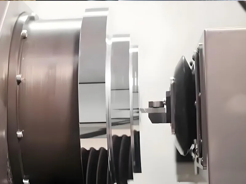
Diamond Turning in Optics
Single-Point Diamond Turning (SPDT) is the cornerstone of modern optical fabrication for non-ferrous metals and IR crystals. Unlike traditional grinding, SPDT uses a mono-crystalline diamond tool with a defined edge radius to shear material at the ductile regime.
Single-Point Diamond Turning (SPDT)
SPDT relies on machine tools with loop stiffness exceeding 500 N/㎛ and resolution of 1 nanometer.
- Kinematics: The process uses air-bearing or hydrostatic oil-bearing spindles to eliminate friction and asynchronous error motion.
- Surface Roughness: We routinely achieve Ra values between 2.0 nm and 4.0 nm on Aluminum 6061-T6 and Oxygen-Free High-Conductivity (OFHC) Copper.
- Tool-Material Interaction: The “cutting” mechanism is actually a high-pressure plastic deformation. The sharpness of the diamond (edge radius < 50 nm) allows chip formation closer to the atomic scale, minimizing sub-surface damage.
Ultra-Precision Capabilities
The capability to hold sub-micron tolerances allows for “Snap-Together” optical assemblies, eliminating the need for active alignment.
- Sub-Micron Accuracy: We control diameter and thickness tolerances to ±1㎛.
- Diffractive Optics: SPDT can generate diffractive kinoforms (step structures) directly onto the lens surface to correct chromatic aberration.
Freeform Tooling
Slow Tool Servo (STS) and Fast Tool Servo (FTS) technologies allow the diamond tool to oscillate synchronously with the spindle rotation (C-axis).
- Applications: This enables the generation of non-rotationally symmetric surfaces like toric lenses, off-axis parabolas, and Alvarez lenses used in VR/AR headsets.
- Complexity: We can machine freeform surfaces with sag deviations of several millimeters while maintaining optical-grade roughness.
Process Parameters
Optimizing process parameters is an exercise in managing the “Theoretical Surface Roughness” equation:
Where $f$ is the feed rate, and R is the tool nose radius. However, real-world factors like material swelling and vibration (“chatter”) complicate this.
- Tool Material: We use natural or synthetic single-crystal diamonds (SCD). The crystal orientation (100 or 110 plane) is selected to maximize wear resistance against specific workpiece materials.
- Spindle Speed: Typically 2,000 to 6,000 RPM. We avoid resonant frequencies of the fixture/part assembly.
- Feed Rate: For finish passes, feed rates are reduced to 1 – 5 ㎛/rev.
- Depth of Cut (DOC): The finishing pass usually removes less than 5㎛ of the material to minimize cutting forces and elastic deformation of the part.
Materials and Applications
Not all materials can be diamond turned. Ferrous materials (steel, stainless steel) cause rapid chemical wear of the diamond (graphitization) due to the affinity between carbon and iron.
Table: Material Compatibility for SPDT at AFI Parts
| Material Class | Specific Materials | Application Notes |
| Non-Ferrous Metals | Aluminum (6061-T6, RSA-6061), Copper (OFHC), Brass, Tin | RSA-6061 (Rapidly Solidified Aluminum) is preferred for mirrors due to fine grain structure (<1µm), which reduces the “orange peel” effect. |
| IR Crystals | Germanium (Ge), Silicon (Si), Zinc Selenide (ZnSe), Calcium Fluoride CaF₂ | Silicon acts brittle; requires high negative rake angle tools to maintain ductile-mode machining. |
| Polymers | PMMA (Acrylic), Polycarbonate, Zeonex (COP) | High thermal sensitivity. Requires strict temperature control (± 0.1℃) during machining. |
| Electroless Nickel | NiP (>10% Phosphorus) | Plated onto steel or aluminum. Provides a hard, amorphous layer ideal for mold inserts. |
AFI Engineering Tip: For steel mold cores, we plate the surface with High-Phosphorus Electroless Nickel. This allows us to diamond turn the nickel layer to optical quality while retaining the structural rigidity of the steel core.
Aerospace and Defense Uses
Diamond-turned optics are important in aerospace and defense. You can make lightweight mirrors and correctors for satellites. They are also used in sensors. High refraction diamond turning makes small, precise optics for LiDAR and imaging. Diamond-turned optics are also used in medical imaging and lighting.
Tip: Diamond turning lowers form error by about 40%. It also cuts peak-to-valley error by 60%. You save time and money and get better accuracy. Fast fabrication with learning control makes high refraction diamond turning even better.
Diamond turning and single-point diamond turning deliver reliable results. Ultra-precision machining and high-refraction diamond turning help you meet modern optical needs.
Precision Polishing for Surface Quality
While SPDT is precise, it leaves a periodic spiral groove (cusp) on the surface, which causes diffraction effects. Precision Polishing is required to remove these tool marks and achieve sub-angstrom roughness.

Polishing Methods
We employ a variety of polishing mechanics depending on the surface figure (flat, spherical, aspheric).
Table: Comparative Polishing Methodologies
| Polishing Method | Material Removal Mechanism | Application Area | Key Process Variable |
| CMP (Chemical-Mechanical) | Chemical passivation layer formation + Mechanical abrasion | Semiconductor wafers, Sapphire, Silicon Carbide | Slurry pH, Oxidizer concentration |
| Magnetorheological Finishing (MRF) | Shear stress via magnetically stiffened fluid | Aspheres, Freeforms, Correcting wavefront errors | Magnetic field intensity, Dwelling time |
| Pitch Polishing | Viscoelastic flow of pitch lap + abrasive rolling | High-precision flats, Reference spheres | Pitch hardness, Slurry viscosity |
| Elastic Emission Machining (EEM) | Atomic-scale chemical interaction (no mechanical load) | X-ray mirrors, Extreme UV optics | Fluid velocity, Nozzle gap |
Magnetorheological (MRF)
MRF is a deterministic sub-aperture polishing process. It uses a magnetic fluid containing carbonyl iron and abrasive particles (cerium oxide or diamond). When exposed to a magnetic field, the fluid stiffens effectively creating a “spot” polisher that conforms to the part’s shape.
- Advantages: Since the removal function is mathematically defined, we can feed an interferometry error map into the MRF machine to specifically target high spots (peaks), correcting form error to ⋋/20.
Deterministic Polishing
Unlike conventional “pad polishing,” where results depend heavily on operator skill, deterministic polishing relies on Computer Controlled Optical Surfacing (CCOS).
- Dwell Time Optimization: The machine calculates how long the polishing tool must stay at every X-Y coordinate to remove the exact amount of material needed to flatten the wavefront.
Integrating Diamond Turning and Precision Polishing
The hybrid approach—Diamond Turning followed by MRF or Post-Polishing—is the gold standard for creating metal mirrors and complex aspheres.
Workflow Steps
- Rough Machining: CNC milling to near-net shape (+0.1mm stock).
- Stress Relief: Thermal cycling to release internal material stresses induced by milling.
- Semi-Finish SPDT: Establishing the optical datum and surface profile.
- Finish SPDT: Generating the final figure with Ra < 5nm.
- Metrology Step: Interferometric map of the surface error.
- Corrective Polishing: Using MRF or localized polishing to remove the residual error and SPDT turning marks.
Achieving Optical-Grade Results
Case Study: Off-Axis Parabolic Mirror (Aluminum 6061-T6)
- Initial SPDT Result: Form Error PV = 0.35㎛, Roughness Ra = 4.2nm.
- Issue: Diffraction grating effect visible from tool marks.
- Correction: Nickel plating followed by SPDT and final Magnetorheological Finishing.
- Final Result: Form Error PV = 0.06㎛ (⋋/10), Roughness R_a = 0.8nm.
Inspection and Maintenance for Surface Quality
At AFI Parts, our metrology lab is environmentally isolated (Temperature 20℃±0.1℃, Humidity 45%±5\%, Vibration Criteria VC-E). Without this control, thermal expansion of the aluminum fixtures would render sub-micron measurements impossible.
Measurement Techniques
We employ a “Trust but Verify” approach using cross-correlation between different metrology instruments.
Table: Metrology Instrumentation at AFI Parts
| Technique | Instrument Model Example | Vertical Resolution | Lateral Resolution | Primary Application |
| Phase Shifting Interferometry (PSI) | Zygo Verifire / 4D Technology | < 0.1nm | Diffraction Limited | Measuring Surface Figure (Flatness/Power) of polished parts. |
| White Light Interferometry (WLI/CSI) | Zygo NewView / Bruker Contour | 0.1nm | ≈0.5㎛ | Measuring Surface Roughness (Rq) and Step Heights. |
| Contact Profilometry | Taylor Hobson Talysurf | 1nm | Stylus Tip Radius (2㎛) | Measuring Aspheric Form and Diffractive Steps where light slopes are too steep. |
| Atomic Force Microscopy (AFM) | Bruker Dimension | 0.05nm | Atomic Scale | Ultra-fine roughness characterization for X-ray optics. |
Measurement Uncertainty & Traceability
A measurement is meaningless without an uncertainty statement. We calculate Measurement Uncertainty according to the GUM (Guide to the Expression of Uncertainty in Measurement).
- Traceability: All master flats and step gauges are traceable to NIST or PTB physical standards.
- Test Uncertainty Ratio (TUR): We ensure our measurement process is at least 4 times more accurate than the tolerance we are checking (TUR≥4:1).
Tool Maintenance
- Handling: Operators wear powder-free nitrile gloves and face masks. Human breath can cause condensation and oxidation on fresh aluminum mirrors.
- Cleaning: We use the “Drop and Drag” method with optical-grade tissues and high-purity Acetone or Methanol to avoid scratching soft metal optics.
Troubleshooting in Diamond Turning and Polishing

Even with state-of-the-art equipment, defects occur. Root Cause Analysis (RCA) is vital.
Surface Defects: Causes and Solutions
- Mid-Spatial Frequency (MSF) Errors:
- Symptom: “Ripples” on the surface that are not the tool feed.
- Cause: Machine vibration, axis servo loop errors, or external noise.
- Solution: Tune PID servo loops, check air bearing pressure, and use damping pads.
- Center “Pip” or Defect:
- Symptom: A nipple or depression at the exact rotation center.
- Cause: The tool height is not exactly set to the spindle centerline.
- Solution: Perform a tool height adjustment, cut, and measure with a white light interferometer. Adjust height by steps of 0.1㎛.
- Comet Tails / Drag Marks:
- Symptom: Streaks behind impurities.
- Cause: Chip packing or poor coolant evacuation.
- Solution: Increase coolant pressure, change nozzle angle, or use a vacuum extraction system (chip suction).
Advanced Adjustments: Adaptive Control
For high-volume production, we implement In-Process Metrology.
- Thermal Compensation: Sensors monitor the machine frame temperature. The controller automatically applies offsets (G-code shifts) to compensate for the linear expansion of the Z-axis.
- Tool Wear Compensation: As the diamond edge wears (truncation), the effective radius changes. We monitor this and update the tool comp parameters dynamically to prevent form error drift.
Conclusion: The AFI Parts Advantage
Achieving optical-grade surfaces is not merely about owning a diamond turning machine; it is about the mastery of the entire manufacturing ecosystem—from material selection and stress relief to nanometer-level programming and metrology.
By integrating Single-Point Diamond Turning with deterministic polishing and validating results through ISO/MIL compliant metrology, AFI Parts delivers components that meet the rigorous demands of the defense, aerospace, and medical sectors. Whether you need a prototype aluminum reflector or high-volume germanium lenses, our engineering team ensures that every photon is managed with precision.
FAQ
Diamond turning helps you make parts very accurately with deterministic control. You can shape optical elements fast. You do not need as much extra polishing. This method helps you meet tough rules for size and shape. It enables the production of aspheric and freeform surfaces that are impossible with conventional grinding.
Real-time compensation lets you fix tool wear and temperature changes right away. By using feedback from capacitive sensors or laser scales, the machine adjusts the tool path in nanoseconds. This keeps your work very accurate. You can make sure every optical element meets strict rules.
Compensation helps you fix mistakes that happen during machining. Even a 0.1°C temperature shift can cause microns of error. This step makes sure your optical elements have the right shape and surface. You can stop expensive errors and keep your work very accurate.
Ultra-precision diamond machined components work for many optical uses, but generally for Infrared (IR) and reflective optics. Materials like glass and steel cannot be directly diamond turned without specialized setups (like ultrasonic assistance). You can use them in imaging, sensing, and laser systems. These parts give you high accuracy and steady results.
You watch your machines and use compensation methods. At AFI Parts, we maintain a closed “metrology loop.” You check your optical elements often. Real-time compensation helps you fix problems fast. This keeps your work within tight limits.
Technology helps you measure, watch, and change your process. Advanced diamond machining uses sensors and software for real-time compensation. This keeps your optical elements accurate and high quality.
Compensation fixes small mistakes during machining. This makes the surface and shape better. You get more accurate optical elements with fewer problems.
You should pick advanced diamond machining for high accuracy and repeatability. It is the most cost-effective way to produce complex optical surfaces in prototype to medium volumes. Real-time compensation helps you meet strict rules. This method lets you make ultra-precision diamond machined components for hard jobs.
