Ultra-high purity aluminum machining helps stop surface contamination in semiconductor equipment. Clean parts and exact work are very important here. Special machining and strong contamination rules help make more good devices.
- High-purity aluminum helps keep resistivity low in careful processes.
- Tiny impurities can break devices, so cleaning is very important.
- Using pure metals makes equipment work better and last longer.
AFI Industrial Co., Ltd knows a lot about precision machining for semiconductor equipment.
Key Takeaways
- Ultra-high purity aluminum is very important for semiconductor equipment. It prevents surface contamination and improves device performance.
- Keeping aluminum very pure lowers the chance of problems in semiconductor devices. Even small impurities can cause big failures.
- Advanced machining methods, such as CNC machining, ensure aluminum parts are precise and clean. This makes semiconductor equipment more reliable.
- Cleanroom environments are very important for machining. They help keep contamination low and protect aluminum parts.
- Regular checks and inspections are very important. They make sure every step in machining is very clean.
- Safe cleaning methods, like ultrasonic and dry ice blasting, remove dirt without hurting the aluminum.
- Good packaging and careful handling stop contamination during shipping. Cleanroom packaging keeps everything clean.
- Following industry rules, like SEMI and ASTM, helps companies keep high quality and safety in making semiconductors.
Table of Contents
Ultra-High Purity Aluminum in the Semiconductor Industry
The semiconductor manufacturing landscape demands uncompromising rigor in material selection and processing. As fabrication nodes scale down to the Angstrom era, the tolerance for particulate and ionic contamination approaches zero. Ultra-High Purity (UHP) Aluminum machining is not merely a manufacturing process; it is a critical contamination control strategy essential for maintaining yield in wafer fabrication equipment (WFE).
Material Purity and Grades
In the context of vacuum chambers, showerheads, and electrostatic chucks, standard aluminum alloys often fail to meet the stringent outgassing and trace metal requirements.
Purity Levels and Standards
The classification of aluminum purity is governed by the concentration of trace elements such as Iron (Fe), Silicon (Si), and Copper (Cu). For semiconductor applications, we distinguish between standard architectural grades and UHP grades using the “N” notation (nines).
- 4N Aluminum (99.99%): Often used for standard structural components within the cleanroom but outside the direct vacuum process path.
- 5N Aluminum (99.999%): Critical for PVD/CVD chamber liners where minimizing heavy metal contamination is vital to prevent dielectric breakdown.
- 6N Aluminum (99.9999%): Utilized in the most sensitive interconnect metallization processes.
Table 1: Technical Specifications of Aluminum Purity Grades for Semiconductor Applications
| Purity Grade | Aluminum Content | Max Total Impurities | Primary Contaminants Controlled (Fe, Si, Cu) | Manufacturing Method |
| 4N | ≥ 99.99% | < 100 ppm | < 50 ppm | Electrolytic Refining (Hoopes Process) |
| 5N | ≥ 99.999% | < 10 ppm | < 5 ppm | Zone Refining / Fractional Crystallization |
| 6N | ≥ 99.9999% | < 1 ppm | < 0.5 ppm | Advanced Vacuum Distillation |
Ref: ASTM B209 Standard Specification for Aluminum and Aluminum-Alloy Sheet and Plate.
These ultra-pure grades are produced through complex metallurgical processes like vacuum distillation and zone refining to strip away volatile elements that could degrade the electrical resistivity or cause electromigration in the final semiconductor device.
Comparison with Standard Alloys
While Aluminum 6061-T6 is the workhorse of general engineering due to its machinability and strength, it contains magnesium and silicon precipitates that can become contamination sources under plasma exposure. UHP Aluminum eliminates these risks.
Table 2: Comparative Analysis: UHP Aluminum vs. Standard 6061-T6
| Feature | Ultra-High Purity Aluminum (1199/High Grade) | Standard Aluminum Alloy (6061-T6) | Impact on Wafer Processing |
|---|---|---|---|
| Purity | 99.99%+ | ~97.9% | UHP reduces mobile ion contamination (Na+, K+). |
| Heavy Metals | Negligible | Cr, Cu, Zn present | Standard alloys pose risks of heavy metal contamination in the transistor channel. |
| Grain Structure | Uniform, controlled grain size | Variable grain boundaries | Uniform structure in UHP allows for better anodization quality and corrosion resistance. |
| Outgassing Rate | Extremely Low | Moderate to High | Low outgassing is crucial for reaching High Vacuum (HV) and Ultra-High Vacuum (UHV) states quickly. |
For engineers at AFI Industrial Co., Ltd, understanding this distinction is vital. We do not simply “cut metal”; we engineer material integrity to ensure that the substrate supports the strict requirements of semiconductor process chambers.
Applications in Semiconductor Equipment
UHP Aluminum is the material of choice for components exposed to harsh plasma environments and corrosive precursor gases.
Common Components and Uses
Vacuum Chamber Bodies: The main structural vessel for Etch and Deposition tools requires high thermal conductivity to manage process temperatures.
Showerheads and Gas Distribution Plates: These components demand micro-drilled holes with zero burrs to ensure uniform gas flow across the wafer.
Sputtering Targets: The source material for physical vapor deposition (PVD) must be chemically pure to deposit high-quality thin films.
Electrostatic Chucks (ESCs): The base plates require exceptional flatness and dielectric strength properties.
Importance of Cleanroom Environments
Semiconductor fabrication plants (Fabs) operate under ISO 14644-1 Class 1 to Class 5 standards. Materials introduced into this environment must exhibit low particle shedding and chemical inertness.
Table 3: Material Performance in Semiconductor Cleanroom Applications
| Property | UHP Aluminum | Stainless Steel (304/316L) | Quartz | Engineering Note |
| Density (g/cm³) | ~2.70 | ~7.90 | ~2.20 | Aluminum offers a high strength-to-weight ratio, reducing the load on robotic handling systems. |
| Thermal Conductivity (W/m·K) | ~237 (Pure) | ~16 | ~1.4 | High thermal conductivity is critical for rapid thermal cycling in process chambers. |
| Machinability | Excellent | Moderate (Work Hardening) | Poor (Brittle) | Aluminum allows for complex geometries (cooling channels) to be machined efficiently. |
| Fluorine Plasma Resistance | Good (with Anodizing/Y2O3 coating) | Poor | Excellent | With proper surface treatment, Al outperforms steel in fluorine-based etch environments. |
At AFI Parts, we leverage these properties to manufacture components that minimize particulate generation and enhance the mean time between cleans (MTBC) for our clients’ equipment.
Surface Contamination Risks in Semiconductor Manufacturing

In the nanometer-scale geometry of modern integrated circuits, “clean” is a relative term. What appears spotless to the naked eye may be laden with “killer defects” at the microscopic level.
Sources of Contamination
Contamination can be broadly categorized into particles, metallic impurities, and airborne molecular contamination (AMC).
Particles and Chemical Residues
Micro-particles: Generated from machining burrs or clothing fibers. A 0.1-micron particle can bridge electrical pathways in a 5nm node transistor, causing a short circuit.
Organic Residues: Hydrocarbons from cutting fluids (coolants), oils, or grease. These residues can carbonize during high-temperature processing, leading to poor adhesion of deposited films.
Metallic Ions: Sodium (Na), Potassium (K), and Iron (Fe) are particularly dangerous. They act as mobile ions within the silicon dioxide gate dielectric, causing threshold voltage shifts and device reliability failures.
Handling and Environmental Factors
The journey of a machined part from the CNC center to the cleanroom is fraught with risks.
- Tribological Transfer: Contact with improper tooling or fixtures can transfer trace metals onto the aluminum surface.
- Environmental Outgassing: Volatile Organic Compounds (VOCs) from improper packaging materials can adsorb onto the clean aluminum surface.
- Humidity and Oxidation: Uncontrolled humidity promotes the formation of unstable aluminum oxides/hydroxides, which are porous and can trap moisture, extending pump-down times in vacuum chambers.
Impact on Yield and Reliability
The correlation between surface cleanliness and fab yield is linear and unforgiving.
Device Failure and Downtime
Surface contamination leads to Dielectric Breakdown and Electromigration issues. For the equipment manufacturer, this translates to unplanned downtime. If a chamber component sheds particles, the entire tool must be taken offline, vented, cleaned, and requalified—a process that can cost tens of thousands of dollars per hour in lost production.
Cost Implications
Cost of Ownership (CoO) is the primary metric for semiconductor Fabs. Components that degrade quickly or introduce contamination increase the CoO significantly.
- Yield Loss: A 1% yield loss in a modern logic fab can amount to millions of dollars in lost revenue annually.
- Scrap Rate: Contaminated parts often cannot be reworked and must be scrapped.
- Reputation: For OEM suppliers, delivering a contaminated part can lead to immediate disqualification from the supply chain.
Ultra-High Purity Aluminum Machining and Cleanliness Control

To mitigate these risks, AFI Industrial Co., Ltd employs a manufacturing philosophy rooted in “Design for Purity.” This involves integrating machining precision with rigorous contamination control protocols.
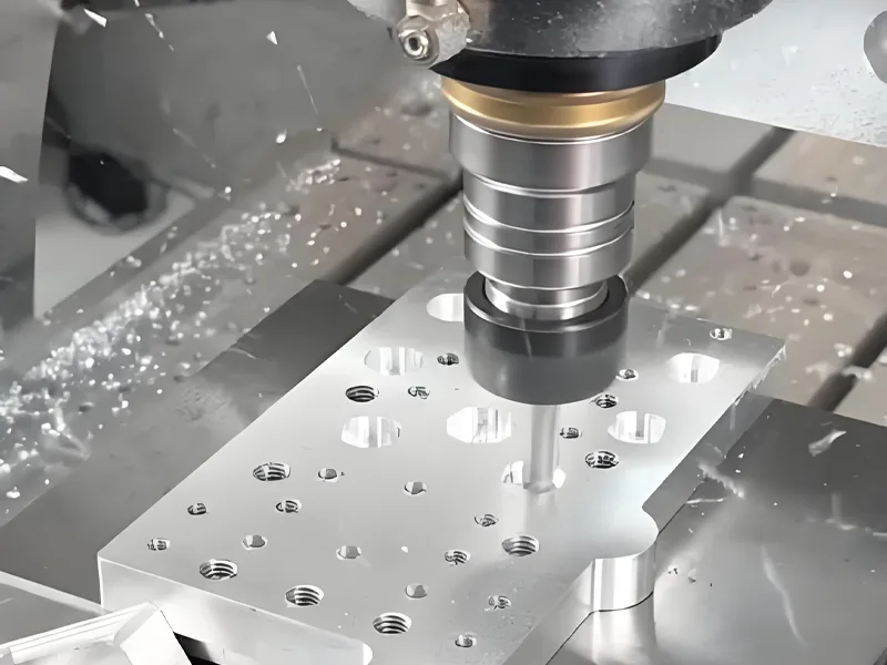
Precision CNC Machining Techniques
Achieving the geometric tolerances required for semiconductor components involves more than standard programming.
Precision CNC Machining
We utilize 5-Axis Simultaneous Milling to machine complex geometries in a single setup. This reduces handling and fixturing, thereby minimizing the risk of contamination and error.
- High-Speed Machining (HSM): Using spindle speeds exceeding 20,000 RPM allows for lower chip loads and reduced cutting forces, minimizing heat generation and thermal distortion.
- Surface Finish: We routinely achieve surface roughness values of Ra < 0.2µm (N4 grade) directly from the machine, reducing the need for post-processing polishing, which can introduce abrasives.
Tool Selection and Maintenance
Tooling is a primary vector for cross-contamination.
- Material Specificity: We utilize Polycrystalline Diamond (PCD) and Monocrystalline Diamond tools specifically dedicated to UHP Aluminum.
- No Ferrous Contamination: Tools previously used on steel or stainless steel are strictly prohibited from touching UHP Aluminum to prevent iron transfer.
- Wear Analysis: Laser tool monitoring systems detect micron-level wear on cutting edges. Dull tools cause “smearing” of the aluminum rather than shearing, creating micro-voids that trap contaminants.
Coolant and Lubricant Management
Standard cutting oils are forbidden.
- Synthetic Water-Soluble Coolants: We use advanced, halogen-free synthetic coolants that are easily removable during the cleaning process.
- Filtration: Coolant systems are equipped with sub-micron filtration to remove recirculating metal fines.
- Control Parameters: We strictly monitor coolant concentration, pH, and conductivity to prevent bacterial growth and chemical attack on the aluminum surface (staining).
Cleanroom Machining Practices
Cleanroom machining is needed to keep everything super clean when making aluminum parts. These steps stop dirt from getting on the parts and keep every surface safe.
Environmental Controls
HEPA Filtration: Our finishing areas are equipped with HEPA filters, ensuring ISO Class 7 or better air quality.
Temperature Stability: The machining center is maintained at 20°C ± 0.5°C to eliminate thermal expansion errors, ensuring dimensional stability for large chamber plates.
Positive Pressure: The room is kept under positive pressure to prevent the ingress of dust from the external factory floor.
Operator Protocols
Human contamination is a significant variable.
- Gowning: Operators wear lint-free cleanroom smocks, bouffant caps, and shoe covers.
- Glove Policy: Only powder-free Nitrile or Latex gloves are permitted. Bare skin contact with UHP Aluminum is strictly prohibited to prevent the transfer of oils, sodium, and salts.
Role of AFI Industrial Co., Ltd in High-Purity Machining
AFI Parts positions itself as a strategic partner in the semiconductor supply chain.
Quality Control Systems
Our Quality Management System (QMS) is integrated with digital traceability.
Table 4: Quality Assurance Framework at AFI Industrial
| Control Measure | Description | Standard/Instrument |
| CMM Inspection | Coordinate Measuring Machines verify geometric dimensioning and tolerancing (GD&T). | Zeiss/Mitutoyo CMM (Resolution 0.1µm) |
| Surface Metrology | Verification of surface roughness (Ra, Rz) and profile. | Profilometer / Interferometer |
| XRF Analysis | X-Ray Fluorescence spectroscopy to verify alloy composition and detect prohibited elements. | Handheld/Benchtop XRF |
| First Article Inspection (FAI) | Comprehensive verification of the initial production part. | AS9102 Standard |
Custom Machining Solutions
We understand that “standard” parts do not exist in semiconductor R&D. Whether it is a prototype showerhead with 0.1mm micro-holes or a large-scale vacuum chamber, our engineering team optimizes the toolpath to balance machining stress, surface integrity, and cycle time.
Preventing Contamination: Best Practices and Protocols
The machining process is only half the battle. Post-process cleaning and surface treatment are where the final purity is defined.

Post-Machining Cleaning Methods
Our cleaning line is designed to remove distinct layers of contamination: gross oils, particulate matter, and surface oxides.
Ultrasonic and Chemical Cleaning
Gross Degreasing: Removal of bulk cutting fluids using solvent-based or aqueous alkaline cleaners.
Ultrasonic Agitation: We employ multi-frequency ultrasonic tanks. Low frequencies (25-40 kHz) remove large particles, while high frequencies (megasonic >400 kHz) are used to dislodge sub-micron particles from blind holes and complex crevices without damaging the substrate.
DI Water Rinse: The final rinse utilizes Deionized (DI) Water with a resistivity of 18 MΩ·cm, ensuring no ionic residues are left on the part.
Dry Ice Blasting
For sensitive components where aqueous residues are a concern, we utilize CO2 Snow Cleaning (Dry Ice Blasting).
- Mechanism: Small CO2 pellets are accelerated towards the surface. Upon impact, they sublime (turn from solid to gas), creating a localized expansion that lifts contaminants away.
- Advantages: It is a non-abrasive, dry process that leaves no chemical residue, making it ideal for cleaning final assemblies.
Surface Passivation
Aluminum naturally forms an oxide layer, but for semiconductor use, this must be controlled.
- Alodine/Chromate Conversion: Provides corrosion protection and electrical conductivity (often used for grounding points).
- Anodizing (Type II & Type III): Creates a hard, non-conductive oxide layer (Al2O3) that is highly resistant to plasma erosion. AFI ensures strict control over pore size and seal quality to prevent outgassing from the anodized layer.
Packaging and Handling for Cleanliness
Packaging preserves the “cleanliness state” achieved during the final wash.
Cleanroom Packaging Materials
UHV Aluminum Foil: Used to wrap ultra-high vacuum parts to prevent hydrocarbon adsorption.
Nylon/Polyethylene Bags: We use Ultra-Clean (UC) grade packaging films that are free from slip agents and amides (Amide-free).
Double Bagging: Parts are double-bagged to allow the outer bag to be removed in the airlock, ensuring only the inner, clean bag enters the customer’s cleanroom.
Controlled Transportation
Shipping containers are robust to prevent shock and vibration, but the internal environment is key. Desiccants and humidity indicator cards are included to monitor environmental conditions during transit to Germany or other international locations.
Inspection and Quality Assurance
Final verification confirms that the part meets the Customer Acceptance Criteria (CAC).
Surface Analysis and Documentation
Visual Inspection: Conducted under high-intensity UV light (Black light) to detect organic residues and fibers.
Water Break Test: A simple yet effective test to verify the removal of hydrophobic oils (ASTM F22).
Particle Counting: For critical applications, we utilize liquid particle counters (LPC) on extraction samples to verify cleanliness levels per ASTM F24 guidelines.
Best Practices Summary
Segregate UHP Aluminum processing from ferrous metals.
Maintain strict coolant chemistry control.
Implement validated cleaning lines with DI water rinsing.
Utilize cleanroom-grade packaging immediately after drying.
Maintain full traceability from raw material ingot to the final shipping document.
AFI Industrial Co., Ltd follows these steps to give very clean aluminum parts that meet the tough needs of the semiconductor industry.
Performance Impact on Semiconductor Equipment
The rigorous application of these protocols directly enhances the performance metrics of our clients’ equipment.

Reliability and Yield Improvements
Reduced Defect Rates
By eliminating micro-burrs and surface particles, AFI’s machined parts significantly lower the Defect Density (D0) on the wafer. In processes like Reactive Ion Etching (RIE), a smooth chamber wall prevents the accumulation of polymer byproducts, reducing the risk of “flaking,” which causes particle excursions.
Consistent Equipment Operation
Process Stability
Consistency in surface finish leads to consistency in process results. For example, the surface roughness of an RF electrode affects the plasma impedance. By maintaining tight Ra tolerances, we ensure that the Plasma uniformity remains constant from chamber to chamber (Chamber-to-Chamber matching).
Longevity and Maintenance Benefits
Extended Component Life
High-quality anodization and surface preparation protect the aluminum from the aggressive chemical attack of Chlorine and Fluorine/oxygen plasmas. This extends the lifespan of consumables, reducing the frequency of parts replacement.
Lower Maintenance Needs
Smoother surfaces are easier to clean during Preventive Maintenance (PM) cycles. This reduces the “Wet Clean” time, allowing the tool to return to production faster, thereby increasing the Overall Equipment Effectiveness (OEE).
Industry Standards and Future Trends
Compliance and Certification
Navigating the regulatory landscape is part of our service.
SEMI, ASTM, and Other Standards
We align our processes with global standards:
- SEMI F19: Specification for the surface finish of components used in high-purity piping and systems.
- ASTM E595: Standard test method for Total Mass Loss (TML) and Collected Volatile Condensable Materials (CVCM) from outgassing.
- ISO 9001:2015 & AS9100: Our quality management systems ensure consistent execution of these standards.
Process Validation and Auditing
We welcome and regularly undergo audits from Tier-1 semiconductor OEMs. These audits validate our Copy Exact (CE!) capabilities, ensuring that a part made today is identical to one made a year ago.
Advances in Precision Machining for Semiconductors
Automation and In-Line Monitoring
AFI is investing in Industry 4.0 technologies.
- In-Process Metrology: Probes integrated into the CNC machine verify dimensions before the part is removed from the fixture.
- Automated Deburring: Robotic deburring ensures 100% consistency in edge breaking, eliminating the variability of manual deburring.
Evolving Purity Requirements
As the industry targets 2nm and beyond, requirements are shifting from “clean” to “atomically precise.” We are researching advanced surface treatments and cleaner alloys to stay ahead of the roadmap, ensuring AFI Parts remains a trusted partner for the next generation of semiconductor innovation.
FAQ
Standard aluminum (e.g., 6061) contains alloying elements like Mg, Si, and Cu that can act as contaminants. UHP aluminum (4N/5N grades) is refined to >99.99% purity to minimize outgassing and heavy metal contamination in vacuum environments.
We use contact profilometers and optical interferometers to measure Ra (Average Roughness) and Rz (Mean Roughness Depth), ensuring compliance with specific engineering drawings, typically achieving Ra < 0.4㎛ or better.
It is a qualitative test used to verify surface cleanliness. If a continuous film of water holds on the surface for a specified time (usually >30 seconds) without breaking into droplets, the surface is considered free of hydrophobic organic contaminants (oils/grease).
Even a perfectly cleaned part can be re-contaminated within minutes if exposed to ambient air. We use nitrogen-purged, double-bagged packaging in a cleanroom environment to maintain the part’s purity until it is installed in the customer’s vacuum chamber.
Yes. Every shipment includes a Certificate of Conformance (CoC) and a Material Test Report (MTR) tracing the material heat number back to the original mill, verifying chemical composition and mechanical properties.
